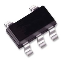
The UCC27517DBVT is a 1-channel High-speed Low-side Gate Driver that can effectively drive MOSFET and IGBT power switches. Using a design that inherently minimizes shoot-through current, UCC27517 can source and sink high peak-current pulses into capacitive loads offering rail-to-rail drive capability and extremely small propagation delay, typically 13ns. The UCC27517 provides 4A source, 4A sink (symmetrical drive) peak-drive current capability at VDD =12V. Internal under-voltage lockout (UVLO) circuitry on the VDD pin holds output low outside VDD operating range. The capability to operate at low voltage levels such as below 5V, along with best-in-class switching characteristics, is especially suited for driving emerging wide band-gap power-switching devices such as GaN power semiconductor devices. It features a dual-input design which offers flexibility of implementing both inverting (IN- pin) and non-inverting (IN+ pin) configurations with the same device.
- 4A Peak source and 4A peak sink asymmetrical drive
- Fast propagation delays (13ns typical)
- Fast rise and fall times (9ns and 7ns typical)
- Outputs held low during VDD UVLO
- TTL and CMOS compatible input-logic threshold (independent of supply voltage)
- Hysteretic-logic thresholds for high noise immunity
- Dual-input design (choice of an inverting (IN- pin)/non-inverting (IN+ pin) driver configuration)
- Unused input pin can be used for enable or disable function
- Output held low when input pins are floating
- Input pin absolute maximum voltage levels not restricted by VDD pin bias supply voltage
- Green product and no Sb/Br
电源管理, 信号处理, 替代能源, 电机驱动与控制


