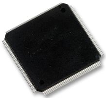
The TMS320VC5509APGE is a Digital Signal Processor based on the TMS320C55x DSP generation CPU processor core. The C55x? DSP architecture achieves high performance and low power through increased parallelism and total focus on reduction in power dissipation. The CPU supports an internal bus structure that is composed of one program bus, three data read buses, two data write buses and additional buses dedicated to peripheral and DMA activity. These buses provide the ability to perform up to three data reads and two data writes in a single cycle. In parallel, the DMA controller can perform up to two data transfers per cycle independent of the CPU activity. The C55x CPU provides two multiply-accumulate (MAC) units, each capable of 17-bit x 17-bit multiplication in a single cycle. A central 40-bit arithmetic/logic unit (ALU) is supported by an additional 16-bit ALU. It supports a variable byte width instruction set for improved code density.
- One/two instruction(s) executed per cycle
- Two arithmetic and logic units (ALUs)
- Programmable low-power control of six device functional domains
- On-chip scan-based emulation logic
- Programmable phase-locked loop clock generator
- USB full-speed (12Mbps) slave port supporting bulk, interrupt and isochronous transfers
- Inter-integrated circuit (I2C) multi-master and slave interface
- Real-time clock (RTC) with crystal input, separate clock domain and separate power supply
- Green product and no Sb/Br
工业, 信号处理


