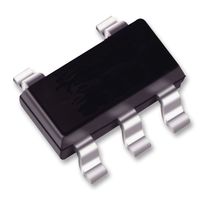


| 型号 | 制造商 | 描述 | 操作 |
| SN65LVDT2DBVT [更多] | Texas Instruments | IC DIFF LINE DVR/RCVR HS SOT23-5 RoHS: Compliant | pbFree: Yes | 搜索 查看资料 |
| SN65LVDT2DBVT [更多] | Texas Instruments | IC DIFF LINE DVR/RCVR HS SOT23-5 RoHS: Compliant | pbFree: Yes | 搜索 查看资料 |
| SN65LVDT2DBVT [更多] | Texas Instruments | IC DIFF LINE DVR/RCVR HS SOT23-5 RoHS: Compliant | pbFree: Yes | 搜索 查看资料 |
| SN65LVDT2DBVTG4 [更多] | Texas Instruments | IC DIFF LINE DVR/RCVR HS SOT23-5 RoHS: Compliant | pbFree: Yes | 搜索 查看资料 |
| 型号 | 制造商 | 描述 | 操作 |
| SN65LVDT2DBVT [更多] | Texas Instruments | LVDS Interface IC Dual LVDS RoHS: Compliant | 搜索 |
| SN65LVDT2DBVR [更多] | Texas Instruments | LVDS Interface IC High Speed Diff Line RoHS: Compliant | 搜索 |
| SN65LVDT2DBVTG4 [更多] | Texas Instruments | LVDS Interface IC DUAL LVDS RECEIVER RoHS: Compliant | 搜索 |
| SN65LVDT2DBVRG4 [更多] | Texas Instruments | LVDS Interface IC DUAL LVDS RECEIVER RoHS: Compliant | 搜索 |
| 型号 | 制造商 | 描述 | 操作 |
| SN65LVDT2DBVT [更多] | Texas Instruments | LVDS Driver/Receiver 0.454V 5-Pin SOT-23 T/R RoHS: Compliant | 搜索 |
| 型号 | 制造商 | 描述 | 操作 |
| SN65LVDT2DBVT [更多] | Texas Instruments | LVDS Driver/Receiver 0.454V 5-Pin SOT-23 T/R (Alt: SN65LVDT2DBVT) RoHS: Compliant | 搜索 |
| SN65LVDT2DBVT [更多] | Texas Instruments | LVDS Driver/Receiver 0.454V 5-Pin SOT-23 T/R (Alt: SN65LVDT2DBVT) RoHS: Compliant | 搜索 |
| SN65LVDT2DBVT [更多] | Texas Instruments | LVDS Driver/Receiver 0.454V 5-Pin SOT-23 T/R - Tape and Reel (Alt: SN65LVDT2DBVT) RoHS: Compliant | 搜索 |
| SN65LVDT2DBVTG4 [更多] | Texas Instruments | LVDS Driver/Receiver 0.454V 5-Pin SOT-23 T/R - Tape and Reel (Alt: SN65LVDT2DBVTG4) RoHS: Compliant | 搜索 |
| 型号 | 制造商 | 描述 | 操作 |
| SN65LVDT2DBVT [更多] | Texas Instruments | LVDS Driver/Receiver 0.454V 5-Pin SOT-23 T/R RoHS: Compliant | 搜索 |
| SN65LVDT2DBVT [更多] | Texas Instruments | LVDS Driver/Receiver 0.454V 5-Pin SOT-23 T/R RoHS: Compliant | 搜索 |
| SN65LVDT2DBVTG4 [更多] | Texas Instruments | LVDS Driver/Receiver 400Mbps 0.454V 5-Pin SOT-23 T/R RoHS: Compliant | 搜索 |
| SN65LVDT2DBVT [更多] | Texas Instruments | LVDS Driver/Receiver 0.454V 5-Pin SOT-23 T/R RoHS: Compliant | 搜索 |
| SN65LVDT2DBVT [更多] | Texas Instruments | LVDS Driver/Receiver 0.454V 5-Pin SOT-23 T/R RoHS: Compliant | 搜索 |
| SN65LVDT2DBVTG4 [更多] | Texas Instruments | LVDS Driver/Receiver 400Mbps 0.454V 5-Pin SOT-23 T/R RoHS: Compliant | 搜索 |
| SN65LVDT2DBVTG4 [更多] | Texas Instruments | LVDS Driver/Receiver 400Mbps 0.454V 5-Pin SOT-23 T/R RoHS: Compliant | 搜索 |
| 型号 | 制造商 | 描述 | 操作 |
| SN65LVDT2DBVT [更多] | Texas Instruments | DIFFERENTIAL LINE DRIVER/RECEIVER SIGNAL
| 搜索 |
| SN65LVDT2DBVT [更多] | Texas Instruments | DIFF LINE DRIVER/RX, 400MBPS, SOT-23-5
| 搜索 |
| SN65LVDT2DBVTG4 [更多] | Texas Instruments | RECEIVER,LVDS, 3.3V, 5SOT23
| 搜索 |
| SN65LVDT2DBVTG4 [更多] | Texas Instruments | RECEIVER,LVDS, 3.3V, 5SOT23
| 搜索 |
| 型号 | 制造商 | 描述 | 操作 |
| SN65LVDT2DBVT [更多] | Texas Instruments |
| 搜索 |
| SN65LVDT2DBVTG4 [更多] | Texas Instruments |
| 搜索 |
| 型号 | 制造商 | 描述 | 操作 |
| SN65LVDT2DBVT [更多] | Texas Instruments | Logic IC Operating temperature: -40...+85 °C Series: SN65LVDT2 Function: Single / LVDS / Receiver Manufacturer: Texas Instruments Package: SOT-23-5 Technology: LVDT
| 搜索 查看资料 |
| 型号 | 制造商 | 描述 | 操作 |
| SN65LVDT2DBVT [更多] | Texas Instruments |
| 搜索 |
| SN65LVDT2DBVT [更多] | N/A |
| 搜索 |
| SN65LVDT2DBVT [更多] | Texas Instruments |
| 搜索 |
| SN65LVDT2DBVT [更多] | Texas Instruments |
| 搜索 |
| 产品描述 / 参考图片 | 制造商零件编号 / 制造商 / 库存编号 | 操作 | ||
| 制造商零件编号: SN65LVDT2DBVT 品牌: Texas Instruments 库存编号: 462-0490 | 搜索 |
| 参考图片 | 型号/品牌 | 描述 / 技术参考 | 操作 |
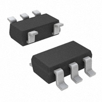 | SN65LVDT2DBVT Texas Instruments | IC DIFF LINE DVR/RCVR HS SOT23-5 | 查价格库存 查看详细 |
 | SN65LVDT2DBVTG4 Texas Instruments | IC DIFF LINE DVR/RCVR HS SOT23-5 | 查价格库存 查看详细 |
| 参考图片 | 制造商 / 说明 / 型号 / 仓库库存编号 | 操作 | |
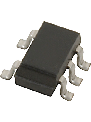 | Texas Instruments Logic IC SOT-23-5, SN65LVDT2, SN65LVDT2DBVT, Texas Instruments 型号:SN65LVDT2DBVT 仓库库存编号:300-22-851 | 搜索 |
| 参考图片 | 型号/品牌 | 描述 / 技术参考 | 操作 |
 | SN65LVDT2DBVT Texas Instruments | IC DIFF LINE DVR/RCVR HS SOT23-5 | 查价格库存 查看详细 |
 | SN65LVDT2DBVTG4 Texas Instruments | IC DIFF LINE DVR/RCVR HS SOT23-5 | 查价格库存 查看详细 |
| 参考图片 | 型号/品牌 | 描述 / 技术参考 | 操作 |
 | SN65LVDT2DBVT Texas Instruments | IC DIFF LINE DVR/RCVR HS SOT23-5 | 查价格库存 查看详细 |
 | SN65LVDT2DBVTG4 Texas Instruments | IC DIFF LINE DVR/RCVR HS SOT23-5 | 查价格库存 查看详细 |
进行最后一道重要生产流程所在的国家

