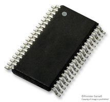
The SN65LVDS108DBT is a 1:8 LVDS Clock Fan-out Buffer. The SN65LVDS108 is configured as one differential line receiver connected to eight differential line drivers. Individual output enables are provided for each output and an additional enable is provided for all outputs. The line receiver and line driver implement the electrical characteristics of low-voltage differential signaling (LVDS). LVDS, as specified in EIA/TIA-644, is a data signaling technique that offers low power, low noise emission, high noise immunity and high switching speeds. The intended application of this device and the LVDS signaling technique, is for point-to-point or point-to-multipoint (distributed simplex) baseband data transmission on controlled impedance media of approximately 100R. The transmission media may be printed-circuit board traces, backplanes or cables.
- One line receiver and eight line drivers configured as an 8-port LVDS repeater
- Enabling logic allows individual control of each driver output, plus all outputs
- Low-voltage differential signalling with typical output voltage of 350mV
- Electrically compatible with LVDS, PECL, BTL, SSTL/HSTL outputs with external termination networks
- Driver outputs or receiver input equals high impedance when disabled or with VCC <1.5V
- 400MHz Clock frequency
- <4.7ns Propagation delay time
- <300ps Output skew
- <1.5ns Part-to-part skew
- <330mW at 200MHz Typical total power dissipation
- Green product and no Sb/Br
时钟与计时, 通信与网络


