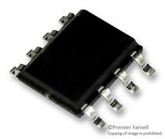
The CDCVF2505DG4 is a high-performance phase-lock loop (PLL) Clock Driver uses a PLL to precisely align, in both frequency and phase, the output clocks (1Y(0-3) and CLKOUT) to the input clock signal (CLKIN). The CDCVF2505 operates at 3.3V. It also provides integrated series-damping resistors that make it ideal for driving point-to-point loads. One bank of five outputs provides low-skew, low-jitter copies of CLKIN. Output duty cycles are adjusted to 50 per cent, independent of duty cycle at CLKIN. The device automatically goes in power-down mode when no input signal is applied to CLKIN. Unlike many products containing PLLs, the CDCVF2505 does not require an external RC network. The loop filter for the PLLs is included on-chip, minimizing component count and space. Because it is based on the PLL circuitry, the CDCVF2505 requires a stabilization time to achieve phase lock of the feedback signal to the reference signal.
- Phase-lock loop clock driver for synchronous DRAM and general-purpose applications
- Spread spectrum clock compatible
- Distributes one clock input to one bank of five outputs
- Three-states outputs when there is no input clock
- Internal feedback loop is used to synchronize the outputs to the input clock
- Integrated RC PLL loop filter eliminates the need for external components
- Green product and no Sb/Br
时钟与计时


