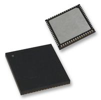
The CDCE72010RGCT is a high-performance low phase noise/low skew Clock Synchronizer that synchronizes a VCXO (Voltage Controlled Crystal Oscillator) or VCO (Voltage Controlled Oscillator) frequency to one of two reference clocks. The clock path is fully programmable providing the user with a high degree of flexibility. The PLL loop bandwidth and damping factor can be adjusted to meet different system requirements. The CDCE72010 can lock to one of two reference clock inputs (PRI_REF and SEC_REF) and supports frequency hold-over mode for fail-safe and system redundancy. The outputs of the CDCE72010 are user definable and can be any combination of up to 10 LVPECL/LVDS outputs or up to 20 LVCMOS outputs. The built-in synchronization latches ensure that all outputs are synchronized for very low output skew. All device settings, including output signalling, divider value selection, input selection and many more, are programmable with the SPI (4-wire Serial Peripheral Interface).
- Two reference clock inputs (primary and secondary clock) for redundancy
- Support with manual or automatic selection
- SPI controllable device setting
- Individual output enables control via SPI interface
- Optional configuration pins to select between two default settings stored in EEPROM
- Efficient jitter cleaning from low PLL loop bandwidth
- Very low phase noise PLL core
- Programmable phase offset (input reference to outputs)
- Wide charge-pump current range from 200μA to 3mA
- SERDES startup mode (depending on VCXO range)
测试与测量, 时钟与计时


