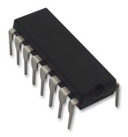
The CD40109BE is a CMOS quad low-to-high voltage Level Shifter will shift a low-voltage digital-logic input signal (A, B, C, D) with logical 1 = VCC and logical 0 = VSS to a higher-voltage output signal (E, F, G, H) with logical 1 = VDD and logical 0 = VSS. It does not require the presence of the high-voltage supply (VDD) before the application of either the low-voltage supply (VCC) or the input signals. There are no restrictions on the sequence of application of VDD, VCC or the input signals. In addition, with one exception there are no restrictions on the relative magnitudes of the supply voltages or input signals within the device maximum ratings, provided that the input signal swings between VSS and at least 0.7 VCC; VCC may exceed VDD and input signals may exceed VCC and VDD. When operated in the mode VCC > VDD, the CD40109BE will operate as a high-to-low level-shifter.
- Individual three-state output capability
- Separately enabled three-state output controls
- Independence of power supply sequence considerations
- Up and down level-shifting capability
- Standardized, symmetrical output characteristics
- 100% Tested for quiescent current at 20V
- Maximum input current of 1μA at 18V
- Green product
信号处理


