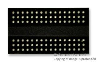
The MT47H128M16RT-25E:C is a DDR2 SDRAM, uses a double data rate architecture to achieve high-speed operation. The double data rate architecture is essentially a 4n-prefetch architecture, with an interface designed to transfer two data words per clock cycle at the I/O balls. A single READ or WRITE operation for the DDR2 SDRAM effectively consists of a single 4n-bitwide, two-clock-cycle data transfer at the internal DRAM core and four corresponding n-bit-wide, one-half-clock-cycle data transfers at the I/O balls. A bidirectional data strobe (DQS, DQS#) is transmitted externally, along with data, for use in data capture at the receiver. DQS is a strobe transmitted by the DDR2 SDRAM during READs and by the memory controller during WRITEs. DQS is edge-aligned with data for READs and centre-aligned with data for WRITEs. The x16 offering has two data strobes, one for the lower byte (LDQS, LDQS#) and one for the upper byte (UDQS, UDQS#).
- VDD = 1.8V ±0.1V, VDDQ = 1.8V ±0.1V
- JEDEC-standard 1.8V I/O (SSTL_18-compatible)
- Differential Data Strobe (DQS, DQS#) Option
- 4n-bit Pre-fetch Architecture
- Duplicate Output Strobe (RDQS) Option for x8
- DLL to Align DQ and DQS Transitions with CK
- 8 Internal Banks for Concurrent Operation
- Programmable CAS Latency (CL)
- Posted CAS Additive Latency (AL)
- WRITE Latency = READ Latency - 1 tCK
- 4 or 8 Programmable Burst Length
- Adjustable Data-output Drive Strength
- 64ms, 8192-cycle Refresh
- On-die Termination (ODT)
- Supports JEDEC Clock Jitter Specification
计算机和计算机周边


