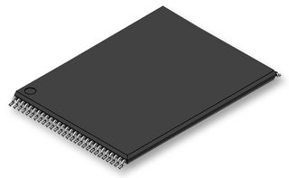
The JS28F128P33TF70A is a 128MB parallel NOR Flash Memory provides high performance at low voltage on a 16-bit data bus. Individually erasable memory blocks are sized for optimum code and data storage. Upon initial power-up or return from reset, the device defaults to asynchronous page-mode read. Configuring the RCR enables synchronous burst-mode reads. In synchronous burst mode, output data is synchronized with user-supplied clock signal. A WAIT signal provides an easy CPU-to-flash memory synchronization. In addition to the enhanced architecture and interface, the device incorporates technology that enables fast factory program and erase operations. The device features a 256-word buffer to enable optimum programming performance, which can improve system programming throughput time significantly to 1.8Mbyte/s. The command user interface is the interface between the system processor and all internal operations of the device.
- High performance - 70ns initial access time
- Asymmetrically-blocked architecture
- Absolute write protection - VPP = VSS
- Power-transition erase/program lockout
- Individual zero-latency block locking
- Individual block lock-down capability
- Password access
- 20μs Typical program/erase suspend
- Basic command set and extended function Interface (EFI) command set compatible
- Common flash interface capable
- Minimum 100000 erase cycles per block
- 65nm Process technology
计算机和计算机周边, 工业, 通信与网络, 消费电子产品


