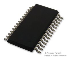
The MAX5183BEEI+ is a dual, 10bit, 40MHz, current/voltage simultaneous output DAC in 28 pin QSOP package. It contains two 10bit, simultaneous update, current-output DAC designed for superior performance in communications systems requiring analogue signal reconstruction with low distortion and low power operation. The MAX5183 provides equal specifications with on-chip precision resistors for voltage output operation. The device is designed for 10pVs glitch operation to minimize unwanted spurious signal components at the output. An onboard 1.2V bandgap circuit provides a well-regulated, low noise reference that can be disabled for external reference operation. It operates in three modes of operation normal, low power standby and complete shutdown which provides the lowest possible power dissipation with 1μA (max) shutdown current. A fast wakeup time (0.5μs) from standby mode to full DAC operation conserves power by activating the DACs only when required.
- Supply voltage range is 2.7V to 3.3V
- Operating temperature range from -40°C to 85°C
- ±2LSB integral nonlinearity and ±1LSB differential nonlinearity
- Wide spurious free dynamic range of 70dB at fOUT = 2.2MHz
- Gain mismatch between DAC outputs is ±0.5% FSR
- Phase mismatch between DAC outputs is ±0.2°
- Low current standby or full-shutdown modes
- Internal 1.2V low noise bandgap reference
- Fully differential outputs for each DAC
信号处理


