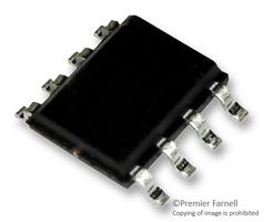
The MAX4017ESA+ is a low cost, high speed, dual, gain of +2 buffer with rail to rail outputs in 8 pin NSOIC package. This high speed closed group buffer has high slew rates, high output current drive and low differential gain and phase errors. It operates from single supply voltage range of 3.15V to 11V or dual supply voltage range of ±1.575V to ±5.5V. The input voltage range extends 100mV beyond the negative supply rail and outputs swing rail to rail. This device requires only 5.5mA of quiescent supply current while achieving 200MHz -3dB bandwidth and 600V/μs slew rate. It is ideal for low power/low voltage applications that require wide bandwidth. Input voltage noise is 10nV/√Hz and input current noise is 1.3pA/√Hz. The MAX4017 is used in battery powered instruments, analogue to digital converter interface and CCD imaging systems.
- High output current drive of ±120mA
- Operating temperature range from -40°C to 85°C
- Internal precision resistors for closed loop gains of +2 or -1
- 0.1dB gain flatness of 30MHz (6MHz minimum)
- Voltage gain of 2V/V, power supply rejection ratio of 57dB at VCC = 5V, VEE = 0V, VOUT = 2V
- Input voltage range extends beyond VEE
- Low differential gain error of 0.04% and differential phase error of 0.02°
- Low distortion at 5MHz, -78dBc spurious free dynamic range, -75dB total harmonic distortion
- Shutdown supply current of 400μA and input bias current of 5.4μA
- Input offset voltage of 4mV at RL = 50 ohm and input offset voltage drift of 8μV/°C
信号处理, 便携式器材, 成像, 视频和目视, 通信与网络, 传感与仪器


