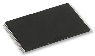
The HY27UF082G2B-TPCB is a 8-bit 2GB NAND Flash IC. The device is offered in 3.3V Vcc power supply and with x8 and x16 I/O interface Its NAND cell provides the most cost-effective solution for the solid state mass storage market. The memory is divided into blocks that can be erased independently so it is possible to preserve valid data while old data is erased. The device contains 2048 blocks, composed by 64 pages. A program operation allows to write the 2112-byte page in typical 200us and an erase operation can be performed in typical 1.5ms on a 128kB block. Data in the page can be read out at 25ns cycle time per byte(x8). The I/O pins serve as the ports for address and data input/output as well as command input. This interface allows a reduced pin count and easy migration towards different densities, without any rearrangement of footprint. Commands, Data and Addresses are synchronously introduced using CE, WE, RE, ALE and CLE input pin.
- Single level cell+single die+large block classification
- High density NAND flash memories
- Multiplane architecture - Array is split into two independent planes
- NAND interface - Address/data multiplexing and pinout compatibility for all densities
- Page size - (2K + 64 spare) bytes and (1K + 32 spare) words
- Copy back program mode - Automatic block download without latency time
- Fast block erase - 1.5ms (typical) block erase time and multi-block erase time (2 blocks)
- Cache read - Internal (2048 + 64) byte buffer to improve the read throughput
- Hardware data protection - Program/erase locked during power transitions
- Data retention - 100000 programs/erase cycles (with 1-bit/528-byte ECC)
工业


